Showing posts with label Electronics. Show all posts

Wednesday 20 December 2017

Ruthenium Monomers: Organic Electronics Beyond Cell Phone Screens

Ruthenium Monomers

Get ready for the age of Organic Electronics

When we think of future we assume of world of better machines, services and futuristic design and appeal taking care of our today’s problems. Organic electronics can help in achieving the very same future we think of with the help of the ruthenium monomers thereby we will get age of carbon based molecules rather than the silicon atoms.

The team behind this research

A team of researchers from the Princeton University, Georgia Institute of technology along with the Humbolt University of Berlin Germany has helped in creating such technology which will pave way for the organic electronics in the future. Their research has already published in the journal named Nature Materials wherein a piece was written on the feasibility in creation of the organic semiconductors.

Organic semiconductors created using this advanced technology backed with ruthenium monomers will help in creating a wide range of flexible electronics in near future. This will also usher an age of emerging technologies ranging from the solar energy conversion to the high quality colour displays which will be seen on the smartphones and other consumers electronics.

How organic semi-conductors are being made?


It is worth noting that the usual semiconductors are made out of silicon which has become a modern found of electronics. It allows engineers to take varied advantages associated with unique properties at controlling the electrical currents. Semiconductors are used across the devices and applications from the computing, switching to signal amplification. They can be found easily in the energy saving devices like the solar cells and the light emitting diodes. To tinker with the ability and functionality of the semiconductors researchers makes use of process called doping wherein a chemical makeup is modified in order to very small amount of impurities or chemical in it.

Organic semi-conductors are developed through using molecular dopants which ensures that it helps in creating highly efficient organic electronic devices. Scientists herein make use of very stable kind of molecular p-dopant which can be easily and successfully deployed in the devices. But so far they had been able to develop such molecular n-dopants which can work with the materials having low electron affinity than the others. The use of the n-doping on the semiconductors has helped in creating high efficiency organic light emitting diode which offers better conductivity than ever before.

What makes the new advanced technology best bet for future?


The best thing about the organic semiconductors is that it can be easily use in the fabrication of flexible devices which will help bringing energy saving products which can optimum functioning at the low temperatures. However the major disadvantage arising from the use of the organic semiconductor that it tends to have a relatively poor electrical conductivity. This disadvantage can result in causing unwanted difficulties in the processes and can even hamper the overall efficiency of the devices. However researchers have started working on improving the electrical properties of the organic semiconductors with ruthenium monomers in order to make them the best option available in the market.

Friday 7 July 2017

Hot Electrons Move Faster Than Expected

 Hot Electrons

Ultrafast Motion of Electrons


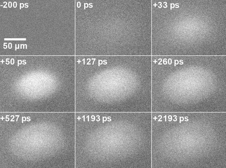
A new research has given rise to solid-state devices which tend to utilise excited electrons. Engineers and scientists at Caltech have for the first time, been in a position of observing directly the ultrafast motion of electrons instantly after they have been excited by a laser. It was observed that these electrons tend to diffuse in their surroundings quickly and beyond than earlier anticipated.

This performance called as `super-diffusion has been hypothesized though not seen before. A team headed by Marco Bernardi of Caltech and the late Ahmed Zewail had documented the motion of electrons by utilising microscope which had captured the images with a shutter speed of a trillionth of a second at a nanometer-scale spatial resolution and their discoveries had appeared in a study published on May 11 in Nature Communications.

 The excited electrons had displayed a diffusion rate of 1,000 times higher than earlier excitation. Though the phenomenon had lasted only for a few hundred trillionths of a second, it had provided the possibility for operation of hot electrons in this fast system in transporting energy and charge in novel devices.

Assistant professor of applied physics and materials science in Caltech’s Division of Engineering and Applied Science, Bernardi had informed that their work portrayed the presence of fast transient which tends to last for a few hundred picoseconds at the time when electrons move quicker than their speed of room temperature, indicating that they can cover longer distance in a given period of time when operated with the help of lasers.

Ultrafast Imaging Technology


He further added that this non-equilibrium behaviour could be employed in novel electronic, optoelectronic as well as renewable energy devices together with uncovering new fundamental physics. Nobel Laureate Ahmed Zewail, the Linus Pauling Professor of Chemistry, professor of physics as well as the director of the Physical Biology Centre for Ultrafast Science and Technology at Caltech, colleague of Bernardi had passed away on 2nd August 2016.

The research had been possible by scanning ultrafast electron microscopy, which is an ultrafast imaging technology initiated by Zewail, with the potential of creating images with picosecond time with nanometer spatial resolutions. The theory and computer models had been developed by Bernardi which clarified the tentative results as an indicator of super-diffusion.

Bernandi has plans of continuing the research by trying to answer the fundamental questions regarding the excited electrons, like how they equilibrate among themselves as well as with atomic vibrations in material, together with applied ones like how hot electrons could increase the efficiency of energy conversion devices such as solar cells and LEDs.

Super Diffusion of Excited Carriers in Semiconductors


The paper has been entitled `Super Diffusion of Excited Carriers in Semiconductors’. Co-authors comprise of former postdoc Ebrahim Najafi of Caltech, who is said to be the main author of the paper and a former graduate student, Vsevolod Ivanov. The research has been supported by the National Science foundation, together with the Air Force Office of Scientific Research, the Gordon and Betty Moor Foundation as well as the Caltech-Gwangju Institute of Science and Technology – GIST, program.

Tuesday 11 April 2017

New Electron Microscope Sees More Than an Image

EMPAD
In the field of material science, electron microscope has lots of application as an effective device. It is usually known to all that this tool helps in viewing at an image. However, with the new enhancement done few days ago, this microscope has gained much more power. And it has been confirmed recently by some physicists at Cornell. The overall system is named as Electron Microscope Pixel Array Detector. It produces image along with some important data on the present electrons, which develop that image.

To give a clear idea about the microscope, Professor David Muller has said that it is possible to identify the tilts, polarity, rotations and magnetic or electric fields.

Manufacturer of the new microscope-

CTL department of Cornell University has accredited the innovation of new microscope to a prominent manufacturer, FEI. According to FEI, the design may be commercialized fully on the present year. In a periodical (Microscopy and Microanalysis) in 2016, the researchers have clarified the work in detail.

In another standard microscope, STEM, the researchers have observed that few electrons could be captured with the help of a specimen. The scanning is done from side to side to generate images. There is a detector at the base, and it interprets how the electrons are varying in their intensity.

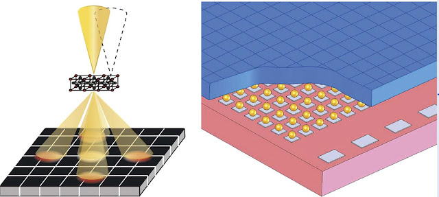
EMPAD is intended for the replacement of a standard detecting system, and it is designed with specific pixels, which are sensitive to electrons. Every one hundred and fifty microns square are attached to a circuit, which warns signals with enough effectiveness in understanding signals. This technology is comparable to what you may find in contemporary camera. The major intention is the detection of angles or directions, where the electrons come out. Every electron usually does not strike at the same pixel.

Microscope with prompt working ability-

EMPAD has remarkable sensitivity and speed along with extensive intensities, tracked by it. It also detects each of the electrons and beams that contain almost millions of electrons. To explicate the phenomenon, Muller has commented that it is just like the act of capturing image of sunset, which displays surface details and everything about the shadows.

The advancement that has been done to the device is really unique and increases the excitements of scientists. Collection of all electrons that are in scattered condition develops the sensitive feature of the device. Moreover, it is also reduces the risk of damage and any negative effect on the living sample. EMPAD has power to track the frame of image within shortest time, and it identifies several electrons for every pixel and frame. In fact, it is multiple speedier than that of any traditional electron microscope.

Thus, the new microscope has brought a revolution in the domain of science. The scientists are now competent at examining the internal part of the cells. The research process has been backed up by Department of Energy in the United States and Cornell. STEM adaptation has also received support from Kavli center.