Thursday 27 August 2015

MIT Unveils 3D Printing Method Using Glass Instead of Plastic


3DGP
They’re calling it 3DGP for Glass 3D Printing.

Borne out of collaboration between the Mediated Matter group at the MIT Media Lab, the Mechanical Engineering Department at MIT, the MIT Glass Lab and the Wyss Institute at Harvard University, 3DGP is the first time transparent glass has been used as precursor, the “ink” in common printing parlance, in 3D printing, also known as additive manufacturing. The paper titled “Additive Manufacturing of Optically Transparent Glass” by Neri Oxman, John Klein et al. will be published in the September 2015 issue of 3D Printing and Additive Manufacturing (3DP+).

  • Using optical glass as precursor in the printing process is a first
The machine works like a conventional 3D printer, where layer upon layer of the precursor is deposited on a work surface, thereby literally building a product from the ground up. In 3DGP, the upper part of the machine is the kiln containing molten glass at up to 1100°C, which is then piped through an alumina-zircon-silica nozzle, which traces the shape to be printed in all three dimensions. The lower chamber anneals the constructed structures.

The process is laser precise and could pave the way for fundamentally changing how glass and related objects are manufactured, the most obvious example being fibre optics, made with higher accuracy and lesser expense, which might be integrated into other surfaces or fabricated materials. This will enable them, for instance, to be incorporated in building construction, such as in precast walls or glass façades, the latter of which can now be created in unimaginable shapes. Also under consideration are printable optoelectronics and photonics.

  •  Printed architectural structures incorporated with fibre optics and optoelectronics a possibility
The accuracy with which the thickness and shape of the glass can be controlled is significant: geometrical variations can be used to generate desired forms of transparency, reflectivity, refractivity and various other properties.

With cutting edge research and indigenous processes and methodology at stake, people are understandably unwilling to reveal the nitty-gritties of the process. Extruder manufacturer Micron3DP, with a similar glass 3D printer in development, has been equally reluctant to share information, except that their printhead can reach temperatures up to 1640°C.

  • Details about the printing process and glass composition are closely guarded
Although the products of 3DGP have only been novelties until now, the group at MIT will soon begin to print various other geometrically complex structures, chiefly those with architectural applications. And like with any case of 3D printing, the bespoke nature of the work means maximum compatibility with each and every application.

Intricate glass work has always remained outside the domain of mechanisation; manual work by master glassblowers has been the way to go. How this new technology might clash with the age-old practice remains unknown. 3D printing might breach new frontiers of adhesion between layers, lack of light distortion, clarity, and most importantly, indistinguishability. Complex patterns created by hand will never be identical to the previous case. 3DGP and its competition do not suffer from this drawback; they can create identical products over and over.

  • Glass-blowing: an art on the way out?
3D printing might also enable creation of new shapes and structures that might have been impossible to fashion by hand, whether due to weight or other restrictions.

New Internet Routing Method Allows Users to Avoid Sending Data through Undesired Countries


Internet_routing
Censorship of information has become quite commonplace all across the world. The developing countries and developed countries- both are using censorship in similar fashion to thwart the flow of information on the online medium. Censorship is even a greatest threat to the open channel communication on the internet. If data travels from the route, which passes by countries, which had placed censorship, then it is a cause of worry for data integrity.

A new system offers sublime internet routing features

Some computer scientists at the University Of Maryland have come up with a commendable solution of advanced internet routing method. A method has been developed which provides a concrete proof to the internet users so that their information does not cross through certain geographical areas, which possess censorship. The advantage of using of this new system is that it can be deployed immediately without wasting any time and it happens to be extremely easier to use and doesn’t require any special or extensive knowledge.

How this new internet routing method works?

This new system of internet routing has been named Alibi Routing and is expected to be presented in the upcoming event of Association for Computing Machinery Special Interest Group On Data Communications (ACM SIGCOMM) in London.

Information when transmitted over the internet in form of website requests or email content then it is broken into different packets and later on it is sent through a series of routers until it reaches its destination. Through the censoring of content, some parts of the world are known to actively engage in modifying the data, which is returned to the users. Alibi Routing uses an extensive peer-to-peer network in order to locate peers- who are running alibi routing software- and relay the user’s packets to the final destination through avoiding the forbidden regions. In this system a peer is termed as “alibi” whose work is to provide proof through calculations whether the information can relay fast at a particular time over a particular geographical location or not. Successful rates show that the information has reached successfully to its desired destination without traversing through the forbidden regions.

Users can use safety parameter in the Alibi Routing in order to get much better control over their data. If a safety parameter is set at larger then it will be hard to find an alibi but at smaller safety parameter alibi can be found easier. The safety parameter shows the user’s desired level confidence whether their data packets are safeguarded from travelling the forbidden regions or not.

Alibi Routing gives better control to users over their data
 
In the recent times, censorship of the internet traffic and information has resulted in the creation of suspicious boomerang routing. This routing makes it easier to monitor the data, which leaves a region to come back again, which is not at good for the end users. Computer scientists have developed the Alibi Routing system in a bid to empower the users to have better control over what happens with their data on the internet.

Wednesday 26 August 2015

Charge Your Phone the Lo-Fi Way

Lo-Fi

Charging Phone – Lo-Fi Way - Nipper

From pocket solar panels and kinetic energy converting armbands to wireless inductive charging docks, portable phone charger market seems to be more like science fiction with each passing day. For those interested in updated lo-fi option or has a backlog of AA batteries around the place, could utilise a gadget known as Nipper which could be of some help.

The Nipper tends to hold in place, two AA batteries with magnets and plugs in the smartphone’s micro USB port in order to deliver extra jolt of power around 10% with 30 minute charge and 20% with one hour charging. It has been developed for the purpose of quick spurts and emergencies instead of full fuel ups and is appropriate for those moments of time when one tends to be trapped in a subway station and to avoid the risk of arrest by plugging into an outlet.

The Nipper is hyper portable measuring around 17mm cubes and fits on a keychain. Presently it only works on phones with micro-USB connectors with models of Samsung, HTC, Nokia and other Android devices. However, the designers are of the opinion that an iPhone compatible option is in the pipeline and the first Nipper would be shipped in April 2016.

Small Phone Charger – Emergency Use

The Nipper is a small phone charger, small enough to be carried around wherever you go and is readily available everywhere – household AA batteries and is primarily designed for emergency use. It is the phone’s smallest phone charger and can be carried anywhere.

When one is in desperate need in using the phone, but is unable to access to the laptops, electrical sockets, wind turbine or solar panels, the Nipper comes to your aid in these situations. When it is not being used, it can be attached to a keychain, pocket or bag and when needed, you can open the Nipper and place two AA batteries between the magnets and connect the same to the phone.

 The Nipper tends to give an extra 10% battery capacity in 30 minutes and 20% in over an hour for a modern smartphone which was tested by utilising a HTC one M7 with Duracell Ultra AA batteries. The power output differs based on the batteries used, in the case of new Duracell batteries; it was found that it gave 500mAh.

Circuit – Boost Converter

The Nipper comprises of 3 neodynium magnets and have the double function of holding the batteries in place while simultaneously makes an electrical connection to the Nipper circuit board. This circuit is known as a boost converter which turns the power from the batteries into a 5v power supply in order to charge the phone.
If the volume of Nipper is small, 3D print of the cases out of high quality nylon will be done but if the demand is high and the need to make a full Nipper army is needed, mold will be injected in the cases out of polypropylene. The two halves of the Nipper can be connected by fabric or genuine leather straps. The neodymium is the nickel plated on the classic Nippers while gold plated on premium Nippers.

The AA batteries are generally recognized and the most widely sold battery and though it does not seems to be sensible relying on AA batteries for daily charging of the phone, it could prove to be handy in times of emergency.

Tuesday 25 August 2015

IBM Announces 7 nm Computer Chip Breakthrough


Chip
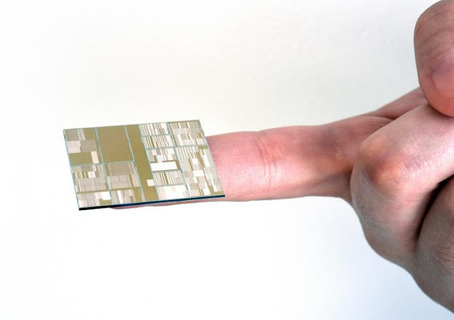
The latest breakthrough in technology seems to have overcome the main issue, which had posed one of the most "grand challenges" of the industry. IBM has created a test version of a semiconductor, which has the ability to shrink down the circulatry. This prototype is the first of its kind in the world. The microchip industry is always evolving and there are better products available in the market every new day. This ever evolving industry has to face immense difficulties due to the extent of their growth and due to various technological and physical limitations. But inspite of all the hindrances IBM has been successful in creating a chip with seven nanometers transistors.

Gradual advancement

The leader of this industry, Intel has been the recipient of several technical hurdles throughout. Technologists have even begun to question one of their foundation theories; they are questioning whether the long withstanding pace of chip improvement, the Moore's Law, could possibly continue beyond the present 14-nanometre generation of chips. Every generation of chip technology can be differentiated with the aid of the least size of fundamental component, which switches the current at nanosecond intervals. Now the advancement in technology has made the transition from the 14 nanometer to the manufacturing of 10-nanometer generation of chips.

Ever-evolving technology

This advanced technology created by IBM is basically an advanced version of the ultradense computer chips which has approximately four times the capacity of the other most powerful chips. As the advancements are brought forward in every generation of the chips, each of them brings forth an estimate of around 50% reduction in the region required by a given amount of circuitry. The new chips created by IBM are suggestive of a possibility that the semiconductor technology shall continue to shrink at least through 2018.

Individual identity

The advanced feature in these chips are the presence of the This advanced technology created by IBM is basically an advanced version of the ultradense computer chips which has approximately four times the capacity of the other most powerful chips. IBM has used silicon-germanium in their chips. In the other variants of chips, pure silicon is used. But IBM instead of using pure silicon has opted for silicon-germanium, which happens to be the key ingredient of the molecular-size switches. This also aids in faster transistor switching and in the lower power requirements.

Yet to be released in the market! 

However, it must be duly noted that most of these are mere speculations and experimentation. Nothing has been launched in the market as of yet. There are numerous complex procedures, which will test whether the product is viable for sale in the market. IBM shall take the final decision in collaboration with their development partners at the State University of New York's Polytechnic Institute in upstate New York. In the previous year, IBM had released a statement, which had declared their 3 billion dollars investment over a time period of five years to forward their chip technology and meet the demands of cloud computing, mobile products, data and other technologies.

Announcing the D-Wave 2X Quantum Computer

D-Wave
D-Wave Systems Incorporation launched the world’s first quantum computer named D-Wave One which was commercially available on May, 2011. It operates on 128-qubit chipset and it uses quantum annealing technology in order to solve optimization problems. Many of the you don’t know what is a Qubit. Qubit is a quantum analogue of bit and it is a unit of quantum information used in quantum computing. It is also referred as quantum bit.

About D-Wave 2X Quantum Computer

D-Wave Systems is the only company based in British Columbia, Canada, known to sell quantum computers worldwide. It recently announced the availability of the new generation of quantum computers, named D-Wave 2X. D-wave 2X will help customers to solve very complex as well as larger problems with its 1000+qubits capacity including other advancements in technology.

Besides having beyond 1000 qubits capacity, it also incorporates other scientific technologies. Advancements include it operates at 15millikelvin temperature, very close to absolute zero. Having 128,000 Josephson tunnel junctions, it consists of most complex superconductor integrated circuits as new processors ever used successfully. Its 50% noise reduction has led to its quicker performance.

Performance of D-Wave 2x

A number of benchmark tests have been done in order to compare it with ordinary PCs to solve optimization problems.

One of the benchmarks is computation time. Computation time needed to solve complex optimization problems with bigger problem size is same for both classical as well as quantum processors. Therefore it becomes prohibitive for the 1000+qubit D-Wave 2x processor to find the optimal solution. Even if optimal solutions are obtained, many large scale solvers tried to find solutions which were close to optimal and they were given a specified time to submit the best solution obtained.

In order to solve hardware problems, D-Wave Systems established Time to Target (TTT) metric. Summary of TTT are given below:
  • Near optimal solutions were found to be 600times faster than usual comparable times by highly skilled solvers. Quantum anneal time is used for this comparision.
  • Using total time measurements D-wave 2x found near-optimal solutions 15x faster than the solvers.
  • The hardware problems are of best performance than software solvers, which is of high advantage by using D-Wave 2x.
  • The difference between optimal and near-optimal solutions is very less around 1% less. But D-Wave 2x works 100x faster to find near-optimal solutions rather than optimal ones.
D-Wave’s product, the 1000+qubit D-Wave 2X quantum computer, is the most technologically advanced efficient quantum computer in the world. It is based on the concept of using a novel type of superconducting processor that takes the help of quantum mechanics to accelerate computation massively. It is the best computer that can tackle complex optimization problems that exist across many domains such as:
  • Optimization
  • Financial Analysis
  • Machine Learning
  • Pattern Recognition
  • Software/Hardware Verification
D-Wave 2x is such a high precision quantum computer that it can evaluate 21000 possible solutions that are converged to near-optimal solutions, thus having more possibilities than the articles that exists in this universe. The powerful effect of quantum computation is not shown by any ordinary computers of any kind that could represent such huge number of possibilities, thus making D-Wave 2x Quantum Computer a cutting edge technology.