Showing posts with label quantum technology. Show all posts

Tuesday 28 August 2018

Uncovering the Interplay between Two Famous Quantum Effects

Quantum Effects

What Happens when two Quantum Effects Combine?

In science, the Casimir effect and superconductivity are well known phenomenon and are widely studied. On their own, scientists know all that is there to study about them. But what happens when two widely known quantum effects combine with each other? Researchers at Delft University have tried doing just that.

By conducting a simple experiment, using a microchip with two wires, scientists plan to observe what happens when two of the most known quantum effects combine. Scientists placed two wires in close proximity to observe the Casimir effect when they become superconducting.

What is the Casimir Effect? 


For us non- scientists, knowing what something like Casimir effect is not really a given. Named after Dutch scientist Hendrik Casimir with Dirk Polder, The Casimir effect was discovered.

When objects are placed very close to one and another, and I mean really close like a thousandth of the diameter of your hair, then you get the Casimir effect.

The minute space or vacuum between these objects pushes the objects together, giving you the Casimir effect.

The same quantum effect is present with all objects, but to get it to work right, the precise space between objects is a must. With Casimir effect, scientists come to know what that exact space in- between is.


What is Superconductivity as one of the Quantum Effects? 


This one too was discovered by another Dutchman. Discovered by Heike Kamerlingh in the early twentieth century, superconductivity describes how certain metals like aluminium and lead conduct electricity at very low temperatures such as at cryogenic ones.

The knowledge of superconductivity has revolutionized the world of physics and has led to many discoveries and inventions such as magnetically levitated trains and MRI scans. Even the mobile stations use the same quantum effect.

So Getting to the point with these two Quantum Effects: 


Scientists know everything that there is to know with these quantum effects. But have never really explored what happens when both these quantum effects combine. That is until now.

Casimir effect has been widely studied with many different objects but never really been used with superconductors as the objects. This was not because no one thought of it but because of technological problems of conducting an experiment at cryogenic temperatures.

What is the solution to observe these two quantum effects at work? 


Researchers at Delft University used a unique sensor that allows them to measure forces acting between two closely spaced superconductors to observe both quantum effects at play.

To observe these two quantum effects at work, scientists used a microchip which is the sensor that houses two wires spaced closely to one and another and that can be cooled to give you superconductivity.

These wires have holes in the middle in which light gets trapped. Any displacement in light shows scientists the forces acting with these two quantum effects.

What did scientist find with these two Quantum Effects? 


Scientists may not have discovered anything new as yet, but have disproved a theory with both Quantum effects.

A theory states that the Casimir effect will be more because of gravitational fields bouncing off the superconductors. Scientists combining both these quantum effects, seen nothing of the sort.

Monday 19 March 2018

Researchers Demonstrate Existence of New Form of Electronic Matter

Electronic Matter
According to the news that has been published in the journal ‘Nature’, engineers based at the University of Illinois have shown that a new form of electronic matter exists. It is called quadrupole topological insulators (QTI).

The properties exhibited by this electronic matter, QTI could bring about a wide range of possibilities in the computer field. It holds great promise in the manufacturing of low-power, robust computers and various devices, that are all defined at the atomic scale.

The topological insulators (TI) are basically electrical insulators on the inside but are conductors along the boundaries. This unique property exhibited by the topological insulators makes them a special type of electronic matter.

A group of electrons form their own phases within the materials. This can be either in the solid, liquid and gas phase, as is seen in water. They can also form an uncommon phase like a topological insulator.

What is this new phase of Electronic Matter? 


The new form of electronic matter is the Quadrupole Topological Insulator. According to theoretical physics, some of the topological insulators have an electrical property known as quadrupole moment.

As we see in a material, the electrons carry a charge. In the process, the material becomes bipolar, that is it contains the positive as well as the negative charge.

Now, in a higher order class of material, we get a quadrupole which is a coupling of two positive and two negative charges. In crystals, the electrons can arrange themselves in such a way that they can give rise to high-order multipoles besides the usual dipole units. In the case of multipoles, four or eight charges are collectively arranged in a unit. The basic forms of multipoles are the quadrupoles wherein two positive and two negative charges are coupled together in a unit.

An analog of a QTI was shown by the researchers of the University of Illinois. They demonstrated it by using a special material from printed circuit boards.

Each circuit has a square of four identical resonators or devices that can absorb electromagnetic radiation at a particular frequency. The boards were positioned in a grid to form the crystal analog.
Each of these resonators behaves like an atom and the connections between the resonators act as bonds between these atoms.

The system is then subjected to microwave radiation to measure the amount that has been absorbed by each of the resonators. This in turn will indicate the behavior of the electrons in an analogous crystal. If the microwave radiation absorbed by a resonator is more, then there are higher chances of finding an electron on the corresponding atom.

In the above experiment it was inferred that the corners of the connected resonators absorbed the microwave radiation at a specific frequency whereas the rest of the units did not do so. The researchers then separated the bottom row from the grid and on subjecting it to the microwave radiation, it was noticed that the next highest rows showed the topological effects on absorbing the radiation.

They concluded that the edges of a QTI are not conductive unlike that seen in a TI. It was only the corners which are active and they correspond to the four localized point charges that form the quadrupole moment.

On measuring the amount of microwave radiation each of the resonators absorbed in the QTI, it was confirmed that the resonant states was in a particular frequency range and localized in the four corners. This shows the existence of predicted protected states that would be filled up by electrons that would in turn form four corner charges.

With the experiment conducted, scientists are beginning to understand the possibilities of the new electronic matter and its application. As of now, the physicists can predict that the new form of electronic matter exists, but no material has been found to have these properties.

Tuesday 9 January 2018

Researchers Chart the ‘Secret’ Movement of Quantum Particles

The secret movement of the quantum particles is a secret no more

Quantum mechanics is a secretive domain which doesn’t give out everything at once rather scientists have to dig deeper to make new discoveries. This time around scientists has been able to come up a theoretical way of mapping the secret movement of the quantum particles which has been done earlier.

It is worth noting that the basic and quite fundamental idea associated with the quantum theory is that all of the quantum objects has the ability exists both like a particle or wave and they don’t even remain present in the manner unless they are being measured. The way quantum objects are present were famously described by Erin Schrodinger through his experiment which asked whether the cat is dead or not dead in the box.

Finding and measuring the quantum objects


Most of scientists assumes that quantum objects remains present in the wave form which helps in using mathematical tool and come up with rational representation of the quantum particles as they appear in the nature. Therefore it was necessary to map or track the secret movement of the quantum particles to know the exact nature of the quantum objects.

Every particle is expected to interact with the environment and when it does so it is registered as a tagging activity. A group of researchers has simply happened to outline a way in which these very tagging interactions can be tracked without even the need of looking at it.

Telepathy is a reality


Earlier quantum scientists put forward the idea that information can easily be transmitted two different persons without even the need of particles moving in between them. It might appear to be a figment of imagination or taken right out of a science fiction fantasy as it strikes just like telepathic connections.

However quantum scientists have a newly coined word for this phenomenon which is called counterfactual communication. The naming of this term is quite unusual as this mode of communication simply goes against long stand way standard way of communication wherein information has to be transferred between two different sources and in order to make it happen ‘particles’ have t move.

Now it is vital to measure this new method of communication and this can only be done through exactly finding where the particles when information is being transferred between the two different objects. The task of pin-pointing the particles in the quantum world isn’t a simple and usual task therefore scientists came up with the tagging method which allowed them to chart the secret movement of the particles in the quantum world. This method only helps in tracking the movement but it give any insight into what particle is doing.

A number of prior research showed that these particles might have the potential to do some non-classical things when they are not being observed and this non-classical thing could be the ability to remain in places at the same time. Using the tagging scientists will be soon uncovering the mystery surrounding the quantum particles when they are not being observed.

Thursday 21 September 2017

Integrated quantum Optical Circuits Soon a Reality

Scientists are on the Verge of Enabling Chip with Quantum Optical Circuit for Information Processing


A group of researchers working on the quantum nano photonics has come up with a method which would result in the development of new age quantum optical circuit. Our world of technology is going through a breakneck pace of advancement which is happening almost every given second across the varied fields. One such field is filled with quantum computers and networks which are designed to work in a way better than our conventional computers and networks.

Our traditional computing devices and networks works by encoding information in binary bits while the quantum computing makes use of quantum bits which can contain two vales at the same time. Quam Computers thus have the ability to process a larger amount of information with lesser number of calculation steps. This functionality makes them a huge potential for the creating energy efficient computation along with sensing and securing the communication in near future.

Developing Quantum Optical Circuit


In order to develop quantum computers researchers will have to get a working circuit to power it. So far researchers have failed to create an effective integrated quantum circuits but it has been finally done by the KTH researchers. This team made use of the novel nano-manipulation technique in order to transfer the selected single photon emitters right into the nanowire present on a silicon chip. This process was utilized to carefully build a highly integrated optical circuit which has the ability to filter single photons as well as multiplex them. This quantum optical circuit makes use of multiple quantum dots in order to generate light in varied colours thereby encoding different information on the same chip.

Developing a fully functional quantum optical circuit it was a challenge to build all of its components deterministically. In other words each and every component of this unique circuit is simply designed and optimized a single specific task. Researchers had to work in a tiresome fashion with no room of error at all in order to get right set of characteristics embedded in its exact location on the circuit.

Achievement And Future Application Of Quantum Optical Circuit


This team of researchers has been able to get achievement associated with their name for years to come. Their work has also resulted in the creation of a hybrid approach which helps in combining two very different semiconductor technologies. Essentially they had combined III-IV technology using their nanowire-based emitters with the silicon technology to create an integrated quantum optical circuit. As stated earlier no one has been able match this feat before using a hybrid integration utilizing just the nanowires.

This intricate process had made them  successful at generating and adding filtered single photons right on the silicon chipset without making use of any external components. Their great invention and complete breakdown of the methods and results will be published shortly in a popular scientific journal named Nature Communications. This also paves the way for the scientists to develop effective quantum circuits in future for specific purposes.

Saturday 10 June 2017

Scientists Demonstrate Microwave Spectrometer Tailored for the Majorana Quest

Majorana

Majorana Particles: The Researchers Quest Pass on to Next Level

A scientific team led by Attila Geresdi to research in Majorana particles has recently paved way to pass the research of the Majorana particle to the next level. They had illustrated a new technology altering certain description for future control of Majorana particles. The Majorana states, unusual quantum particles, only survive under very special condition.

While in theory projected in 1938, the researcher team of Leo Kouwenhoven inm 2012 were determined for the first time in a chip. The key constituent is a nanowire ariled by a superconducting part’, states Attila Geresdi, directing researcher of the study.

These magical particles are the structure blocks of topological quantum computation, a bright path in quantum technology that is chased by various research groups in cooperation with Microsoft.

The topological quantum bits are as such bastioned from faults, that means that if you execute a quantum procedure, it ever works. In the road towards the quantum computing based on Majorana particles there are big obstacles on the way to face, but this recent great work open the grand doors to a new program of quantum experiments. Through this new method both primal physics and scientific challenges towards the activity of Majorana states can be explored.

The Quest for Majorana Particles

The Majorana particles, named after Ettore Majorana, are used in elementary particle physics to mathematically describe fermions (i.e., particles with a half-numbered spin) when they are equal to their own antiparticles: so-called majorana fermions.

This property implies that the particles described must not bear any electrical charge. The researchers across the globe has great quest for this Majorana particles which are the building blocks for the topological quantum computer. Generally, the realization of this Majorana particles is quite difficult as they exists only in a very particular circumstances. Majorana research through Nanowires

Semiconductor nanowires represent an interesting research area at the interface between basic research and technology. Analysis of the growth process, properties and possible applications is part of the research on semiconductor nanowires.

Successive semiconductor nanowires have been successfully produced and characterized by various growth methods in the electron microscope. Further studies, e.g. Of the electrical and optical properties are currently being carried out. The superconducting propinquity phenomenon in semiconductor nanowires has newly alter the work of new superconducting edifice.

The researchers across the globe in colloboration with Microsoft are conducting researches to find out the Majorana using the Nanowire covered with a super conducting layer. Fortunatly the team of researchers found that the Majorana states only rely on measuring of electron flow through Nanowires.

The Delft research team joined hands with scientists from Yale University combines a Nanowire to a Microwave Spectrometer which does not disturbs Majorana's in any manner. The researchers across the globe are greatly facing hurdles on the research for Topological quantum computing.

But, this wonderful work of the researchers has paved way and pass quantum computing to the next level. This amazing work of these researchers can be found at Nature Physics.


Friday 18 December 2015

Google Says It Has Proved Its Controversial Quantum Computer Really Works

Quantum_Computer

Google’s Controversial Quantum Machine- Quicker than Conventional Computer


Google has informed that it has proof of a controversial machine bought in 2013, can use quantum physics to work through a kind of math which is critical to artificial intelligence and much quicker than a conventional computer. Governments together with leading computing companies like Microsoft, Google and IBM are putting in efforts in the creation of quantum computers due to which the improbability of quantum mechanics in representing data could unlock huge data crunching powers.

Computing giants are of the opinion that quantum computers can make their artificial intelligence software more commanding, unlocking scientific leaps in the field of materials science.

 NASA is expecting that quantum computers could be helpful in scheduling rocket launches and feign future missions as well as spacecraft. Rupak Biswas, director of exploration technology at NASA’s Ames Research Centre in Mountain View, California has commented that `it seems a disruptive technology which could change how we do everything. At media briefing at the research centre, Biswas had commented, regarding the agency’s work with Google on a machine which the company had bought in 2013 from Canadian start-up D-wave systems that it is the world’s first commercial quantum computer.

Superconducting Chip –Quantum Annealer


The computer has been installed at NASA’s Ames Research Centre in Mountain View, California, operating on data utilising superconducting chip known as a quantum annealer. Quantum computer is hard coded with system fitted to what is known as optimization problems that are common on machine learning and artificial intelligence software.
But in the case of D-Wave’s chips it seems to be controversial among quantum physicists and researchers in and out of the company have not been capable of proving that the devices could tap into quantum physics in competing with conventional computers. The leader of Google’s Quantum AI Lab in Los Angeles, Hartmut Neven, had stated recently that his researchers had delivered some firm proof of that.
 They had set up a series of races between the D-Wave computers that was installed at NASA against a conventional computer with a single process. He commented that `for a specific carefully crafted proof-of-concept problem, they had achieved a 100 million-fold speed-up.

Bug in D-Wave Design


A research paper describing the results online had been recently posted by Google though it has not been formally peer-reviewed. Neven had stated that the journal publication would be coming up soon. The results of Google were striking though if they were verified, would only represent fractional evidence for D-Wave. 
The computer which had lost in the contest with the quantum machine had been running a code that solved the problem at hand utilising a system to the one that was in the D-Wave chip. A substitute system is known which could have enabled the conventional compute to be more competitive or win by exploiting what Neven has called a `bug’ in D-Wave design.
Neven had stated that the test which his group had staged tends to be still important since that shortcut would not be available to the regular computers when they tend to compete with the future quantum annealers with the potential of working on larger amounts of data.
A physics professor at the Swiss Federal Institute of Technology, Zurich, Matthias Trover had said that making that to come true could be crucial if chips like D-Wave are to be useful. It would be essential to explore if there are issues where quantum annealing has advantage over the best classical systems and to identify if there are classes of application problems, where these advantages could be realized.

Tuesday 8 September 2015

Quantum Dot Technology May Help Light the Future

OSU

Quantum Dots – New Generation LED Lighting

Developments at the Oregon State University, in the manufacturing technology for quantum dots could soon lead to new generation of LED lighting.Quantum dots are nanoparticles which could be utilised in emitting light and by accurately controlling the size of the particle and the colour of the light.

They have been utilised for some time and can be expensive, lacking optimal colour control. The manufacturing technique that have been developed at OSU would be able to increase to large volumes for low-cost commercial applications providing new ways of offering the accuracy essential for better colour control.

This could create a more user friendly white light while utilising less toxic material together with low cost manufacturing procedures which tend to take advantage of simple microwave heating. It would help the country in reducing its lighting bill in half.

Compared to the cost of incandescent as well as fluorescent lighting and the cost, performance and environmental improvements could eventually create solid state lighting systems which consumers prefer and help the nation in reducing its lighting bill by half, according to researchers.

Same technology could also be merged in improved lighting display, computer screens, televisions, smart phones and the other systems.

Applied to Various Products & Technologies

Significant to the advances that had been published in the Journal of Nanoparticle Research, is use of both a continuous flow chemical reactor and microwave heating technology that is theoretically identical to the ovens which are part of every modern kitchen.

The constant flow system tends to be fast, cheap, energy efficient and would cut manufacturing costs. Microwave heating technology could report a problem that had held back wider use of these systems, so far, which is the accurate control of heat needed during the procedure.

Microwave approach would translate into development of nanoparticles that are exactly the right size, shape and composition. According to an associate professor and chemical engineering in the OSU College of Engineering, Greg Herman, states that `there are various products and technologies that quantum dots can be applied to but for mass consumer use, possibly the most important is improved LED lighting.

Eventually they would be able to manage in producing low cost, energy efficient LED lighting with the soft quality of white light which people would want and at the same time the technology would use nontoxic materials and reduce the waste of materials which are used and translates to lower cost and environmental protection.

Research Supported by Oregon BEST/National Science Foundation

According to Herman, some of the top existing LED lighting being produced presently at industrial levels tend to use cadmium which is highly toxic and the system now being tested and developed at the OSU depends on copper indium diselenide which is a much more benign material with high energy conversion efficiency.

Some earlier systems creating these nanoparticles for use in optics, electronics and biomedicine tend to be slow, expensive and at times toxic as well as often a waste. There is also a possibility of other applications of these systems. Cell phones and portable electronic devices could use less power and could last longer on a single charge.

`Tuggants or compounds with certain infrared or visible light emissions could be utilised for accurate and prompt identification which include control of counterfeit bills or products. OSU has been working with private sector in the development of this technology. The research is being supported by Oregon BEST and the National Science Foundation Centre for Sustainable Materials Chemistry.

Saturday 29 August 2015

A Little Light Interaction Leaves Quantum Physicists Beaming


Light
A remarkable research conducted by a group of physicists had brought insightful revelations where it is possible to make building block of the quantum computer with the use of pure light. This team of physicists comes from University of Toronto and they had successfully published their paper in the Nature Physics on ‘logic gateway’ an essential segment of computer circuitry.

What are logic gate? 

Logic gates segments are designed to execute operations on the input data in order to create outputs. In the earlier times during the phase of classical computers, the diodes or transistors formed the logic gates but with the advancement of quantum computer component it is now comprised of both the individual atoms as well as subatomic particles. Processing of information as per the laws of the quantum physics usually takes place when these particles interact with each other.

In the quantum computing the light particles are known as ‘photos’ and offers various advantages but it is extremely difficult to invoke interaction among them in a profitable manner. The research conducted by the physicist from University of Toronto is centered on finding successful ways of creating such interactions.

Researchers are upbeat with their experiment results

One of the paper’s authors Aephraim Steinberg had shed some amazing insight on the experiment results. Physicists at the University Of Toronto had studied the effect of photon on an optical beam but they had advanced their experiment in a wholesome fashion. In usual conditions, light beam passes through each other without causing change on effect on the other. In order to effectively develop technologies such as optical quantum computers it is necessary to make beams interact with one another. But no one had achieved feat with using just single photon.

How this experiment was conducted? 

The researchers had conducted this experiment of creating light beams interaction in a delicate process of two steps. A shot of single photon was forced at the rubidium atoms so that it iced to a millionth of a degree above absolute zero. Later on the photons become intertwined with the atoms and this resulted in rubidium interaction to another optical beam. The photon started changing the atom’s refractive index which brought a minute but calculable “phase shift” in the beam. This method used in the experiment can be actively brought into use in the optical quantum logic gate, which will facilitate input-output and information-processing.

Where this experiment can be applied? 

The best place to use this experiment in wholesome application is in the quantum logic gates. This advanced process will help in seeing the interactions in a new manner and in the study of optics a new filed will be revealed. Currently the researchers are working further to answer two important questions i.e. what happens when dealing with one particle of light at time and how differently the light beams will interact with other. Researchers are hopeful of finding these essential questions answers soon with continuous research and experimentations.

Tuesday 25 August 2015

Announcing the D-Wave 2X Quantum Computer

D-Wave
D-Wave Systems Incorporation launched the world’s first quantum computer named D-Wave One which was commercially available on May, 2011. It operates on 128-qubit chipset and it uses quantum annealing technology in order to solve optimization problems. Many of the you don’t know what is a Qubit. Qubit is a quantum analogue of bit and it is a unit of quantum information used in quantum computing. It is also referred as quantum bit.

About D-Wave 2X Quantum Computer

D-Wave Systems is the only company based in British Columbia, Canada, known to sell quantum computers worldwide. It recently announced the availability of the new generation of quantum computers, named D-Wave 2X. D-wave 2X will help customers to solve very complex as well as larger problems with its 1000+qubits capacity including other advancements in technology.

Besides having beyond 1000 qubits capacity, it also incorporates other scientific technologies. Advancements include it operates at 15millikelvin temperature, very close to absolute zero. Having 128,000 Josephson tunnel junctions, it consists of most complex superconductor integrated circuits as new processors ever used successfully. Its 50% noise reduction has led to its quicker performance.

Performance of D-Wave 2x

A number of benchmark tests have been done in order to compare it with ordinary PCs to solve optimization problems.

One of the benchmarks is computation time. Computation time needed to solve complex optimization problems with bigger problem size is same for both classical as well as quantum processors. Therefore it becomes prohibitive for the 1000+qubit D-Wave 2x processor to find the optimal solution. Even if optimal solutions are obtained, many large scale solvers tried to find solutions which were close to optimal and they were given a specified time to submit the best solution obtained.

In order to solve hardware problems, D-Wave Systems established Time to Target (TTT) metric. Summary of TTT are given below:
  • Near optimal solutions were found to be 600times faster than usual comparable times by highly skilled solvers. Quantum anneal time is used for this comparision.
  • Using total time measurements D-wave 2x found near-optimal solutions 15x faster than the solvers.
  • The hardware problems are of best performance than software solvers, which is of high advantage by using D-Wave 2x.
  • The difference between optimal and near-optimal solutions is very less around 1% less. But D-Wave 2x works 100x faster to find near-optimal solutions rather than optimal ones.
D-Wave’s product, the 1000+qubit D-Wave 2X quantum computer, is the most technologically advanced efficient quantum computer in the world. It is based on the concept of using a novel type of superconducting processor that takes the help of quantum mechanics to accelerate computation massively. It is the best computer that can tackle complex optimization problems that exist across many domains such as:
  • Optimization
  • Financial Analysis
  • Machine Learning
  • Pattern Recognition
  • Software/Hardware Verification
D-Wave 2x is such a high precision quantum computer that it can evaluate 21000 possible solutions that are converged to near-optimal solutions, thus having more possibilities than the articles that exists in this universe. The powerful effect of quantum computation is not shown by any ordinary computers of any kind that could represent such huge number of possibilities, thus making D-Wave 2x Quantum Computer a cutting edge technology.

Thursday 8 January 2015

Fraud-Proof Credit Cards Through Quantum Physics


Credit_Cards
Researcher at the Eindhoven University of Technology and the University of Twente have come up with a secure way to authenticate he credit cards, IDs and biometrics with quantum cryptography. It is the method of quantum secure authentication through optical keys, which consist of sending a beam of light at cards with very special paint and later the reflection will use as the authentication mechanism.

It involves the coherent states of light with photon number, which means there are a lot of spaces for the bouncing of photons, as it can be more than one space on same time, so whenever the credit cards reflect the beam with specific paint there will be more dots or points of light will sent back than there are photons and it is well known that attackers won’t have enough amount of data to measure the entire pattern.

Research Details: 

This solution is very easy in implementation with current technology and it doesn’t depend on claim of researcher and stored data. In the process of research experts used the cards coated with millions of nano-particles in the form of white paint, which help to bounce the incoming light particles. In research experts have used the two spatial light modulators, a photon detector and a pinhole. In the process one of SLM have transformed incoming light on to desired challenge wave-front to sent it on the card and the reflected response with challenge were stored in a database.

In process each response of pair will requires 20 KB of memory or for 2,500 pairs it will require 50-MB of database and correct response were sent to a lens behind, which will be behind second SLM that focused them onto a photon detector to authenticate them.

System details: 

High spatial dimension states with photons are the main challenges for system. The created patterns will depend on the challenge as well as the position of the paint particles. In experiment each challenge was described by a 50 x 50 binary matrix, where every element corresponding to a phase was either 0 or Pi. As per the lead researcher, “All we need to make the illumination pattern complex to make sure that number of photons are lower than the number of pixels, which appears in image.

The first SLM will transform the wavefront of an incoming plane into a selected challenge wavefront at random from of database. As the challenge is created dynamically and exists only after the transformation, so it cannot be intercepted. All the response will be recorded in a phase-sensitive manner.

Nothing is impossible: 

When it comes to the failure of experiment, so system can be brake with the help of passive linear optical system, which can automatically transforms the any challenge into the correct response and it is very close to make the physical copy of key. So for full proof security must be done in the patterns of layers as different patterns require different level of security.

Tuesday 16 September 2014

Now Take Photos in Complete Darkness with Quantum Camera


Quantum Camera
Now low light is no disadvantage for Cameras as they are getting innovated to take better images even in low light. With this theory Researchers of University of Glasgow have got the inspiration and they are working towards creating an image that will be capable of working even with less than 1 photon per pixel. This team has been able to achieve this milestone which was seemingly impossible through combination of two esoteric technologies namely compressive imaging and photon heralding. The process involves seems to be very clear and simple leaving aside the amount physics and math that went under it.

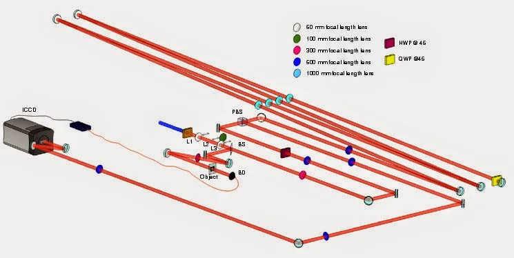
The first part of this peculiar science is heralded imaging. Also known as “ghost imaging”, this is based on heralded photons. Spontaneous parametric down-conversion (SPDC) process can be used to produce pairs of quantum-entangled photons under certain situations and then they can be split apart. At most of the time, if one of the photon is detected even the other one gets detected.

How the imager works? 

The imagers utilizes a beam splitter which send one out of each pair of photons it has created through the object that needs to be imaged and through a highly sensitive single-pixel detector. The other pair goes through high-speed camera. When a photon is sensed through a target object it leads to the activation of the detector. After this the detector send signal for shutter to open up for about 15 nanoseconds. This amount of time eliminate all the background noise and record the position of the second heralded. This allows it to take the picture of the photons quickly. A delay of 70 nanoseconds has been added to the path of the camera which allows enough time for the shutter to release signal to camera from detector.

Although one can’t avoid the shot noise which comes from the Poisson distribution of photons, this kind of heralded photons enables the imager’s light requirement get as low as one photon per pixel. Compression imaging is used to deal with this noise and go further which is less than one photon per pixel. Compressive imaging utilizes frequency domain information by relying on inherent redundancy of information in natural subject.

Advantages: 

So Quantum camera can take photos in complete darkness and it will need only one photon per pixel. This amazing camera is not meant only for show purposes. The research team hopes it will drive the growth of cameras for scholarship researches, wherein they are required for investigating and analyzing subjects which are extremely light sensitive, for example certain kind of biological specimens. So when it comes to complete darkness, it’s time to ditch all the high end cameras with limited functioning in darkness and move ahead to the next generation of Camera- Quantum Camera.