Thursday 17 August 2017

Atomic Movies May Help Explain Why Perovskite Solar Cells Are More Efficient

Perovskites – Cheap/Easy/Flexible 

Perovskites has taken the solar cell industry by storm in recent years. They tend to be cheap, easy in producing as well as flexible in their applications.

Moreover their efficiency in converting light into electricity has developed quicker than that of any other material from under 4% in 2009 to over 20% in 2017, where some of the experts are of the belief that Perovskites Solar Cells could ultimately outperform the most common solar cell material, silicon. However, irrespective of their reputation, researchers are not aware why perovskites solar cells tend to be so efficient.

Research had been carried out with powerful `electron camera’ at the Department of energy’s SLAC National Accelerator Laboratory which has now revealed that light whirls atoms around in perovskites, potentially explaining the high efficiency of these next –generation solar cell materials as well as provides clues in making improved ones.

 Aaron Lindenberg from Stanford Institute for Materials and Energy Sciences – SIMES and the Stanford PULSE Institute for ultrafast science that had jointly operated by Stanford University and SLAC, had stated that they have taken a step towards resolving the mystery.

He further added that they had recorded movies which tend to show that certain atoms in a perovskite seem to respond to light within trillionths of a second in a very unusual manner.
Perovskite Solar Cell
 

Flexibility Based on Atomic Structure of Material

 
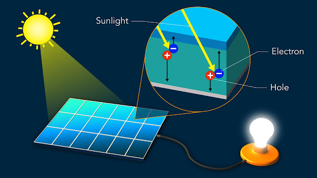
This could facilitate the transport of electric charges through the material and enhance its efficiency. The study had been published recently in Science Advances. When light is said to shine on perovskites solar cell material, its energy tends to displace some of the negative charged electrons of the material.

This is inclined to leave behind `electron holes’ having positive charge where the electrons had initially been located. Electrons and holes tend to migrate in opposite sides of the material thereby developing a voltage which could be utilised to power electrical devices. The efficiency of perovskites solar cell seems to depend on how freely electrons as well as holes tend to move in the material.

In turn, their flexibility is based on the atomic structure of the material. In silicon solar cells for instance, silicon atoms is said to line up in an orderly manner within crystals as well as the smallest structural defects tend to reduce the ability of the material to harvest light efficiently.

As a consequence, silicon crystals need to be grown in costly multistep process under very clean conditions while perovskites are said to be produced with the combination of chemicals in a solvent that tends to evaporate to leave an extremely thin film of perovskite material according to the study’s lead author from SIMES at SLAC, Xiaoxi Wu.
Perovskite Solar Cells
 

Lower Cost/Lightweight

 
He further added that simpler processing would mean lower costs and unlike silicon solar cells, perovskite thin films seems to be lightweight as well as flexible and can be applied with ease to virtually any surface. With regards to perovskites what is it that permits some of them to harvest light in an efficient manner?

Scientists are of the opinion that one of the keys is how their atoms tend to move in reaction to light. In order to get a better understanding, Wu together with his colleagues researched on these motions in a prototype material made of iodine, lead together with an organic molecule known as methylammonium.

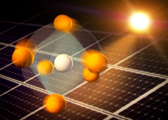
 The iodine atoms tend to be arranged in octohedra, eight-sided structures which seems like two pyramids that is joined towards the base. The lead atom tends to sit inside the octohedra and the methylammonium molecule is between octohedra.

The architecture seems common to several of the perovskites investigated for perovskites solar cell applications. The earlier research could have explored mostly the role of the mehylammonium ions together with their motions in transporting electric charge through the material.
 

Light Cause of Huge Deformation in Network

 
Wu had stated that they had found that light is the cause of huge deformations in the network of lead and iodine atoms which tend to be crucial for the efficiency of perovskites. At the Accelerator Structure Test Area – ASTA of SLAC, the researchers had initially hit a perovskite film which was less than two millionths of an inch thick having a 40-femtosecond laser pulse.

One femtosecond is said to be a millionth of a billionth of a second and in order to determine the atomic response, they directed a 300-femtosecond pulse of highly energetic electrons via the material and noticed how the electrons had been deflected in the film. This system known as ultrafast electron diffraction – UED enabled them to reconstruct the atomic structure. The speedy improvement of perovskite solar cells has enhanced them in the photovoltaics world as well as of high interest to the academic community.

While the operational system seems to be comparatively new, there are possibilities of additional research in the basic physics and chemistry regarding perovksites. Moreover, from observations of past two years, the engineering development of perovskite formulation together with the fabrication sequences has given rise to significant increases in power conversion efficiency.

Monday 14 August 2017

Energy Storage Solution Combines Polymers and Nanosheets

Energy Storage

Fresh Lightweight Composite Material – Energy Storage 


According to a team of Penn State scientists a fresh lightweight composite material for the purpose of energy storage in flexible electronics, electric vehicles and aerospace application has experimentally revealed energy storage at operating temperatures beyond present commercial polymers.

The said polymer-based ultrathin energy storage material can be produced utilising techniques which are already being used in industry. Professor of materials science and engineering, Penn State, Qing Wang had stated that this is part of a series of work which had been done in the lab on high temperature dielectrics for use in capacitors.

 Prior to this work they had developed a composite of boron nitride nanosheets and dielectric polymers, though had realized that there had been significant issues with scaling that energy storage material up economically’. The defining challenge for several of the new, two-dimensional energy storage materials that are being established in academic labs is scalability or making advanced materials in commercially significant quantities for devices.

Wang has mentioned that `from a soft material perspective, 2D materials are fascinating though how to mass produce them is a question. Moreover, being able to combine them with polymeric materials is a key feature for future flexible electronics applications and electronic devices’.

Functional Dielectric Device-


In order to resolve this issue, his lab collaborated with a group at Penn State operating in two-dimensional crystals. Nasim Alem, assistant professor of materials science and engineering as well as a faculty member in Penn State’s Centre for 2-Dimensional and Layered Materials had stated that the work had been conceived in conversations between his graduate students, Amin Azizi together with graduate student of Dr Wang, Matthew Gadinski. He further informed that this was the first strong experiment wherein a soft polymeric material together with a hard 2D crystalline material had come together in order to develop a functional dielectric device.

Azizi who presently is a post-doctoral fellow at University of California, Berkeley and Gadinski, a senior engineer at DOW Chemical had generated a technique utilising chemical vapour deposition in order to make multilayer, hexagonal boron-nitride nanocrystal films to transfer the films to both areas of a polyetherimide (PEI) film.

Thereafter they bonded the films together by utilising force on the three-layer sandwich structure. In the outcome which was surprising to the researchers, pressure itself without the need of any chemical bonding had been adequate in making a free-standing film essentially strong to potentially be manufactured in a high-throughput roll-to-roll process.


Hexagonal Boron Nitride – Wide Band Gap Material


In a recent issue of the journal Advanced Materials in a paper titled `High-performance Polymers Sandwiched with Chemical Vapour Deposited Hexagonal Boron Nitrides as Scalable High-Temperature Dielectric Materials’, the results had been reported. Hexagonal boron nitride is said to be a wide band gap material having high mechanical strength.

 Its wide band gap tends to make it a worthy insulator, protecting the PEI film from dielectric breakdown at high temperatures, the cause for failure in the other polymer capacitors. Above 176 degrees Fahrenheit, at operating temperatures, the prevailing best commercial polymers begins to lose its efficiency though hexagonal-boron-nitride-coated PEI tends to function at high efficiency at above 392 degrees Fahrenheit.

The coated PEI seems to be stable for over 55,000 charge-discharge cycles in testing even at high temperature. Wang has mentioned that `theoretically all these high performance polymers which seem to be so commercially valuable could be coated with boron nanosheets in order to block charge injection. He further added that he is of the opinion that this would make this technology feasible for forth-coming commercialization.


Supported – U.S. Office/National Science Foundation 


Alem has also commented that there are several devices that are made with 2D crystals at the laboratory scale; however the defects tend to make them an issue for manufacturing. With the help of huge band-gap material such as boron nitride, it tends to do a good work in spite of the fact that small microstructural features could not be perfect.

 The first-principles calculations resolute that the electron barrier recognized at the interface of the PEI/hexagonal boron-nitride structure as well as the metal electrodes practical to the structure for the purpose of delivering current was said to be significantly higher than typical metal electrode-dielectric polymers contacts, thus making energy storage materials more complex for charges from the electrode to get injected into the film.

This task had been done by the theoretical research group of Long-Qing Chen, Professor of Materials, Science and Engineering, professor of engineering science and mechanics as well as mathematics – Penn State, Donald W. Hamer. Several others contributing to this work comprise of post-doctoral scholar Qi Li as well as graduate student Feihua Liu in the lab of Wang, undergraduate Mohammed Abu AlSaud in the lab of Alem, senior scientist Jianjun, Wang, post-doctoral scholar Yi Wang together with graduate student Bo Wang who were all from the Chen group at that point of time. This work had also been supported by the U.S. Office of Naval Research as well as the National Science Foundation.

Saturday 12 August 2017

Samsung Galaxy S8 Active Leak Shows Lot of Compromises

Samsung Galaxy S8

New Leak: Samsung Galaxy S8, shows a lot of compromises

The next Samsung top model Galaxy S8 will come in two versions, but this does not affect the edge of the screen. After some leaks in the past days and weeks, the two S8 variants comes together.

At the Mobile World Congress last week, the Samsung Galaxy S8 and the large version Galaxy S8 +, yet the next flagship of the Koreans is the theme of the hour. If you are interested in the MWC, please contact us.

Fingerprint sensor of the Galaxy S8

The goal is to integrate the fingerprint into the display. Samsung's decision to relocate the fingerprint sensor to the back of the device with its upcoming smartphone Galaxy S8 has not caused much joy for a number of users. The solution, which is also preferred by the company, but technically did not manage.

"Samsung has put a lot of resources into the technology presented by Fingerprint specialist Synaptics last year, but the results were frustrating," South Korean economic magazine The investor cited to the informed source. The result is the displacement of the sensor on the backside next to the camera.

5.7 and 6.2 inches

Now you can still sleep your curiosity in terms of the sizes of the two S8 models, because on the side SlashLeaks (via The Verge) a picture has appeared, which shows the two smartphones side by side. The smaller is, of course, the conventional Galaxy S8, which brings a 5.7-inch screen, next to the 6.2-inch version can be seen.

The data on the two screens are unconfirmed, but it is apparent that customers will actually get a lot of display for their money. Because 5.7 inches is diagonal, which was previously reserved for the Galaxy Note 7.

Samsung Galaxy S8

Source of the current Leaks is a manufacturer of screen protectors. Technical data, the current Leak has not been tested yet.

Samsung will offer a Snapdragon 835 or an Exynos 9 Series 8895, depending on the market, as a chipset. In addition, four gigabytes of RAM and a QHD display with an (unusual) aspect ratio of 18.5: 9.
Chance for Apple

Synaptics had officially launched its on-screen technology last December. This should not have been too late. But the process suggests that the supplier leaned too far out of the window and the technology could not meet the quality requirements of Samsung.

This is, of course, the chance for Apple to grab. The competitor is also in charge of the device. Until the presentation of the next Apple smartphones goes so a few months into the country, which can be of course decisive, in order to get quality necessary for a market maturity of the technology.

Friday 11 August 2017

Automatic Toothbrush That Takes Just 10 Seconds To Clean Your Entire Mouth

First Fully Automatic Toothbrush

An unusual automatic toothbrush which could help the user in the early hours of the morning in cleaning their teeth and remove plaque in only 10 seconds will be coming up shortly. It is said to the first fully automatic toothbrush in the world. Its patent pending device which brushes all the teeth at once is totally automatic and completes the cleaning in only ten seconds.

All that is needed is to press a single button, wait for ten seconds and the user will have perfectly clean teeth. All the units of Amabrush seem to be equipped with a sound and light indicator which enables to signal several diverse information regarding the prevailing battery status, finished tooth-brushing sessions, flaws, together with other scenarios.

Moreover, their specifically formulated toothpaste has been provided in big bottles together with more durable as well as steady reusable toothpaste capsules. This would be economical in saving shipping fees as well as the complete cost for the user. According to its manufacturers, the brush seems like a bristly mouth guard that has the tendency of dispensing toothpaste and vibrates in order to clean every tooth. With the worldwide shipping beginning in December, customers can now pre-order the device for £70 ($90).

Bacteria-Resistant Silicone – 3D Bristles

In order to utilise the device, the user can put the toothbrush in their mouth and press on a button to begin the cleaning procedure. The system is said to utilise tailored toothpaste capsule that comes at a price of £2.60 ($3.40) and tends to last for around a month.

The manufacturers of this brush had stated that the device has been made from bacteria-resistant silicone featuring 3D bristles on both the sides. According to its inventors, the material is said to be adequately soft to avoid gum disease though hard enough to clean the teeth. They have also informed that since the material tends to be flexible, one type of size would be appropriate for both men as well as women.

The device is said to send out tough vibrations having amplitude of 9.5G, utilising a process to differ the waves of vibrations. The creators had mentioned on Kickstarter that `even in 10 seconds, every tooth surface has been cleaned longer compared with common brushes. If one brushes their teeth for the recommended 120 seconds with a regular toothbrush, every surface tends to get brushed for just 1.25 seconds.

Tooth-Brushing Less Troublesome

They have further added that Amabrush tends to brush all your surfaces for the whole of 10 seconds. The toothbrush would be required to be replaced once in two to three months in order to be effective as per the makers.

It accomplishes all the recommended methods where the bristles are aligned in a 45° angle against the line of the gum and are said to be adequately soft to rub rather than to scratch. Moreover the pressure against the teeth seems to be quite light and the subtle vibrations are said to move the bristles back and forth enabling them to eliminate the plaque, while keeping the gums from getting damaged.

It has been created to make tooth-brushing less troublesome where some may tend to hate brushing their teeth and may not brush the areas which need to be cleaned. Some may not be inclined in brushing correctly. The purpose of focus is – right tooth-brushing for one and all which is done automatically.

The Computer That Know What Humans Will Do Next

AI

Computer Code – Comprehend Body Poses/Movement

A fresh computer code tends to provide robots with the possibility of an improved understanding of humans around them, making headway for more perceptive machines from self-driving cars to investigation. The new skill enables the computer to comprehend the body poses as well as movements of various people even to the extent of tracking parts as tiny as individual fingers.

Though humans tend to communicate naturally utilising body language, the computers tend to be somewhat blind to these interactions. However, by tracking the 2D human form and motion, the new code is said to improve greatly the abilities of the robots in social situations.

A new code had been designed by the researchers at Carnegie Mellon University’s Robotics Institute by utilising the Panoptic Studio. The two-story dome has been equipped with 500 video cameras developing hundreds of views of individual action for a specified shot. Recording of the system portrays how the system views the movement of humans utilising a 2D model of the human form.

Panoptic Studio – Extraordinary View of Hand Movement

This enables it to trail motion from the recording of video in real time, capturing everything right from the gestures of the hand to the movement of the mouth. Besides this, it also has the potential of tracking several people at once.

Associate professor of robotics, Yaser Sheikh had stated that they tend to communicate mostly with the movement of the bodies as they tend to do with their voice. However computer seems to be more or less blind to it. Multi-person tracking gives rise to various challenges to computers and hand detections is said to be more of an obstacle.

The researchers, in order to overcome this, utilised a bottom-up approach localizing individual body area in an act. Thereafter the areas were associated with certain individuals. Though the image datasets on the hand of the human seemed quite restricted than those on the face or body, the Panoptic Studio provided extraordinary view of hand movement.

 A PhD student in robotics, Hanbyul Joo had stated that a distinct shot provides 500 views of individuals hand and also automatically interprets the position of the hand.

2D to 3D Models

He further added that hands tend to be too small to be interpreted by most of the cameras, but for the research they had utilised only 32 high-definition cameras though were still capable of building a huge data set. The method could ultimately be utilised in various applications for instance helping to enhance the ability of self-driving cars to predict pedestrian movements.

 It could also be utilised in behavioural diagnosis or in sports analytics. Researchers would be presenting their work CVPR 2017, the Computer Vision and Pattern Recognition Conference, from July 21 -26 in Honolulu. Up to now they have released their code to several other groups in order to expand on its skills.

Finally, the team expects to move from 2D models to 3D models by using the Panoptic Studio in refining the body, face and hand detectors. Sheikh had mentioned that the Panoptic Studio had boosted their research and they are now capable of breaking through various technical barriers mainly as a result of the NSF grant 10 years back.