Showing posts with label IBM. Show all posts

Monday 15 January 2024

IBM Will Train You in AI Fundamentals - For Free

IBM Will Train You in AI Fundamentals - For Free

The AI Fundamentals program of IBM is made inside its SkillsBuild learning portal. There are a total of six courses, and the credentials will take about 10 hours to complete across 6 courses. IBM contributes unique solutions and strategies to lead an evolution in corporate citizenship. These solutions and strategies help to transform & empower the global communities.

IBM Will Train You in AI Fundamentals - For Free

IBM discussed the difficulties of balancing technology with great ethical responsibility. The major topics are:

  • the five pillars of AI ethics,
  • the importance of fairness and avoiding bias, and
  • AI systems have to be transparent against attacks.

The things emphasized by the session via data minimization & differential privacy are:

  • Governance,
  • The protection of personal data, and
  • The significance of privacy.

Artificial Intelligence Fundamentals Learning Plan:

This learning plan enables you to explore the history of artificial intelligence. Then, you get to learn how it is capable of changing the world. In today's world, artificial intelligence helps to make predictions. Also, it is capable of making predictions, understanding pictures and language & learning using circuits inspired by the human brain. After a hands-on simulation where you create & test an ML model, you get to know about how to find your career in artificial intelligence.

Introduction to Artificial Intelligence (1 hour 15 mins):

Artificial intelligence has already experienced three waves of transformative development. In recent times, AI is capable of providing the most powerful tools in order to analyze complex data. The function of these tools is to find meaning and learn without human intervention. This course lets you know the history of artificial intelligence. Also, you will be able to explore ways that it is capable of shedding light on unstructured data.

Natural Language Processing & Computer Vision (1 hour 30 mins):

You may already know that a few artificial intelligence systems analyze human language and identify visual pictures. Also, they can make original art. However, do you have any knowledge regarding how these systems do it? If you do this course, you get to explore the theory of natural language & vision processing. Also, you can learn the way technologies drive real-world mechanisms like chatbots & photo analysis.

Machine Learning And Deep Learning (2 hours):

This course is based on how machines learn and make awesome predictions. In this course, you get the chance to explore the actual logic based on which computers learn something. After that, you can learn about new ways through which AI systems are able to solve difficult issues.

Run AI Models with IBM Watson Studio (1 hour and 45 mins):

This course lets you use IBM Watson Studio, which helps you practice how to create an AI machine-learning model in a series of simulations. It is hands-on time, which lets you perform actual work with AI.

AI Ethics (1 hour and 45 mins):

Sometimes, artificial intelligence-based systems misinterpret data or suggest solutions reflecting human prejudice — you could have heard about the issues. If you see real-world examples, you get to know about AI ethics. Also, you can learn the way they are implemented. You can also learn why AI ethics are valuable when it comes to building reliable AI systems.

Your Future In AI: The Job Landscape (1 hour):

Are you one of those who are thinking of a future career in artificial intelligence? When you learn this course, you will be informed regarding the rapid growth of the AI job market. Also, you get to know the skills that are necessary to succeed in this field. While you get to know how real professionals got their start, you are also able to find resources & learning chances, which will help you to work alongside them.

A lot of people around the world have been inspired by artificial intelligence. However, AI has provoked several questions about how it is likely to impact the world of work. We can see the change happening very quickly. According to research from IBM’s Institute for Business Value, executives who estimate almost 40% of their workforce have to reskill over the next three years because of AI &

It is required to address the challenge of equipping the workforce with the skills to achieve success in the future. It is crucial that each person gets an equal chance to participate & thrive. That's why IBM recently announced a new commitment. They will give training to two million learners in AI in 3 years. Their focus is mainly on underrepresented communities.

As equitable access is the main focus, they are ensuring that everyone including even those who have been left behind during the old technological advances, gets benefits from the latest developments in AI.

Free Course Offerings In Generative AI For Everyone:

IBM experts developed AI education, and this free education program, IBM SkillsBuild, helps learners across the world to get benefits from AI education. Their aim is to offer the newest things in cutting-edge technology developments. 

These courses are designed to build on each other. Therefore, learners are able to deepen their understanding the more they go along. After completing the entry-level learning plan, "Artificial Intelligence Fundamentals" comprising 6 courses, learners could earn a digital credential. This program allows learners to explore how AI understands language & images. Also, the learners get to know how AI learns using Deep Learning, neutral networks which can simulate the human brain.

IBM SkillsBuild courses are designed in a way that they become interactive. As a learner, you are able to build an ML model and run it with IBM Watson Studio in one hands-on simulation. A new generative AI roadmap is announced beyond the fundamentals. It includes:-

  • new coursework on Prompt-Writing,
  • Getting Started with Machine Learning,
  • Improving Customer Service with AI and
  • Generative AI in Action.

However, remember that AI doesn't only mean to be smart with technology. It's also about building trust as well as developing models. When you complete the course, you will receive IBM-branded digital credentials, recognized by Potential employers.

Using AI to Improve the Learner Experience:

You can have a better learning experience because of the AI features within IBM SkillsBuild. With the help of AI-powered solutions, students' aptitudes, in which they are interested and their accomplishments are analyzed. Then, they propose credentials to pursue. When you begin your educational journey, you will get a learning path that is generated by artificial intelligence. It depends on your personal choices, experiences, & academic level. Chatbots will support the learners throughout the journey. AI technologies are used in different ways in order to make IBM SkillsBuild better. With the help of AI, the feedback from learners can be reviewed, and the performance of the program is analyzed.

Expanding AI Skills Training Through Partnerships:

While online courses are available to everyone, IBM partners with different organizations worldwide play an important role to increase the reach of skill training. Local partners help in equipping learners from underrepresented backgrounds to help them to learn how to succeed in this career. For example, IT Experience in the United States works with women, Black & other minority communities in the technology sector so that they can get the opportunity to improve their skills and gain experience. 

Celebrating Longevity in Broadcasting:

In Broadcasting, it is important to celebrate longevity. The reason is that it highlights the experience & knowledge which are brought by the professionals. Also, it shows that they are capable of adapting to changes in technology and the industry.

IBM’s AI Fundamentals Training:

Now you know that IBM is offering a free 10-hour AI fundamental training program, and it will start this year. The program is specially designed for those people who want to learn AI in depth. This training program will inform you about the ethics lessons on the importance of AI's responsible use. Once you complete the program, you will get a certificate of completion.

Like IBM's training program, LinkedIn is offering a similar AI training program. Microsoft and LinkedIn call this program Essentials AI training. However, to access the learning portal of LinkedIn, a membership is required. If you are interested, you can go to IBM's Skills Build learning portal to benefit from the training programs. And the same happens for LinkedIn's learning portal. If you are someone who wants to get smart on AI & make informed decisions about the implementation of it, then these are good to go. In order to know more about the training program, you should go to the IBM website.

Certificate of Completion:

Once you complete the program, you will receive a certificate of completion. You can use this to demonstrate your newly acquired knowledge. No matter whether you are an IT professional or a person thinking that AI could change your career — this IBM program is available to everyone who is willing to learn about AI. So, interested people can navigate IBM's Skills Build learning portal to sign up.

The Bottom Line:

Artificial intelligence comes with the potential to make work better for all. But remember that people have to get it right. In order to meet the challenges of the workforce in the future, it is essential to acquire AI skills for everyone. IBM SkillsBuild helps to turn this game-changing technology into a tool which works for the betterment of as many people as possible.

Frequently Asked Questions

Can you learn artificial intelligence for free?

The free online course, which is available to everyone, is called

‘An Introduction to AI’. It lets you learn about AI and other related things.

Is IBM skills free?

SkillsBuild, an online platform that comes with more than 1,000 courses, was launched by IBM. These courses are based on several topics, including artificial intelligence to cybersecurity, data science, cloud & software development. The best thing is these courses are free as well as available in twenty languages, such as English, French, German, Spanish, Ukrainian, and so on.

Does IBM have training for freshers?

As soon as your academic and practical courses are completed, freshers will get the chance to become corporate trainees as well. Credentialing with IBM Training as well as Certifications are an excellent way to demonstrate the skills.

Saturday 10 March 2018

IBM CIMON: IBM Ships Robotic Head to the International Space Station

IBM Cimon

IBM gets into the delivery of equipment to International Space station

International Space Station needs a consistent of supply of essential equipment and food supplies from the earth. Earlier Elon Musk’s SpaceX played a vital role in delivering supplies to the ISS but now even IBM is in the same fray. IBM is aiming towards delivering a very unusual eleven pound robot head to the International Space Station using a device called IBM Cimon or the Crew Interactive Mobile Companion.


All you need to know about IBM Cimon


IBM Cimon is powered by company's popular supercomputer Watson. But IBM is utilizing it in a different manner which enables to embark on a unique mission to the International Space Station. Earlier IBM has used the Watson technology to run a number of crystal experiments as well as solving the Rubik's Cube. IBM is working closely with a German Astronaut named Alexander Gerst in order to use the IBM Cimon to perform variety of tasks like conducting complex medical experiment just using the on-board camera.

IBM Cimon isn't just every tech piece rather the company wishes to establish it as a reliable companion for the astronaut in the space which can do a number of tasks on its own or with little guidance from the astronauts. With IBM Cimon astronauts will be able to get a number of prescribed tasks done with effortless co-ordination on the space station. Secondly IBM Cimon will also act as a safetyimprovement device by giving out timely warning of any impending failure. It will be smart and intuitive enough to find the failure even before it is shown on the astronauts control boards.

IBM Cimon learns and improves on its own


As IBM Cimon is backed with the AI technology this device can literally act as the first space assistant which will be beneficial for the astronauts working on the International Space Station.The use of technology in IBM Cimon allows it to possess speech, text and other image processing capabilities. Secondly it will be smart enough to retrieve certain specific information and finding when needed to offer valuable insight in time of need. Thirdly astronauts will be able to teach a number of skills to the IBM Cimon individually thereby enhancing it application.

IBM is essentially making use of the Watson speech and vision technologies in order to make CIMON recognize and understand the different voice sample with perfection. Visual Recognition of Watson is employed to understand as well as learn the construction of plans of the Columbus module of the International Space Station.

As IBM Cimon will be deployed at the International Space Station it is necessary that it understand its layout so it can move around with ease and simplicity. Astronauts have even taught him a number of procedures which is ought tobe carried out by him in connection with the on-board experiments. IBM Cimon shows that the science fiction wouldn't be a fiction anymore as we move towards creating intelligent robots to assist astronauts in space.

Friday 27 May 2016

IBM Scientists Achieve Storage Memory Breakthrough

IBM

IBM Research – Latest Memory Technology – Phase-Change-Memory –PCM


Scientist at IBM Research, have for the first time demonstrated reliably storing 3 bits of data for each cell utilising a latest memory technology called phase-change memory – PCM. The existing memory landscape tends toextentfrom respected DRAM to hard disk drives to universal flash. However in the last several years PCM has attracted the attention of the industry as a probable universal memory technology based on its mixture of read/write speed, non-volatility, density and endurance.

For instance PCM does not lose data when it tends to power off unlike DRAM. The technology could endure at least 10 million write cycles in contrast to an average flash USB stick that tends to top out at 3,000 write cycles. The break-through of the research has provided quick and easy storage in catching the exponential growth of data from the mobile devices as well as the Internet of Things.

IBM scientists tend to envisage standalone PCM together with hybrid application that would unite PCM and flash storage together with PCM as an exceedingly fast cache. For instance the operating system of a mobile phone could be stored in PCM permitting the phone to launch within a few seconds. In the initiative space, the complete database can be stockpiled in PCM for fast query processing for time-critical online application like financial transaction.

Two Stable States – Amorphous/Crystalline


Machine learning processes utilising huge datasets would see a rapid boost on reducing the latency overhead while reading the data between iterations. The PCM materials tend to display two stable states, namely the amorphous – without a clearly defined structure and crystalline – with structure phases, of high and low electrical conductivity, respectively. Scientists at IBM and the other institutes had successfully demonstrated the potential to store 1 bit per cell in PCM earlier. However, presently at IEEE International Memory Workshop in Paris, for the first time, the IBM scientists are presenting, successfully stored 3 bits per cell in a 64k-cell array at higher temperatures and after a million endurance cycles.

 Dr Haris Pozidis, author of the paper and the manager of non-volatile memory research at IBM Research – Zurich had informed that `phase change memory was the first instantiation of the universal memory with properties of DRAM and flash, thus answering one of the grand challenges of the industry.

Novel Coding/Detecting Scheme Employed


He further added that reaching three bits per cell seems to be a significant milestone since at this density, the cost of PCM tends to be significantly less than DRAM and nearer to flash. In order to attain multi-bit storage, IBM scientists had developed a couple of innovative enabling technologies, a set of drift-immune cell-state metrics and drift-tolerant coding with detection schemes.

The new cell-state measure a physical property of the PCM cell more precisely, which tends to remain stable over a period of time and are hence insensitive to drift, affecting the stability of the electrical conductivity of cell with time. In order to provide extra strength of the data stored in a cell over ambient temperature fluctuation, a novel coding as well as detecting scheme had been employed.

The scheme tends to adaptively change the level threshold which is used in detecting the stored data of cell so that they follow variation owing to temperature changes. The outcome is that the cell state can be read reliably over long period of time after the memory is programmed and hence offers non-volatility.

Friday 9 October 2015

IBM Breakthrough Improves Carbon Nanotube Scaling Below 10nm

nanotube

IBM – Beneficial Scaling Abilities in Carbon Nanotubes


IBM has invested a great amount of time and effort in researching carbon nanotubes – CNTs in the past few years. The presence of single walled carbon nanotubes together with their marvellous semiconductor properties happened independently at NEC as well as at IBM with Big Blue being interested in capitalizing on the discovery for over a decade.

Researchers at IBM published a paper wherein they claimed to have demonstrated extremely beneficial scaling abilities in carbon nanotubes. Discussions were on, regarding the difficulties of scaling semiconductors since the distance between features tends to contract with each passing generation.

However the specific breakthrough which IBM tends to claim is in an area of chip design and not much has been discussed over it. In the case of conventional silicon, a known problem as semiconductors tends to shrink and the contact area from the metal and semiconductor has not been scaling.

Smaller contact area, generally lead to increased resistance which means higher heat. Manufacturers have battled against these developments with various methods. However the lack of contact scaling seems to be one of the main barriers in pushing silicon to ever smaller sizes.

Carbon Nanotube Technology – Solution to Problem


IBM is of the opinion that its carbon nanotube technology could solve that issue. EETimes has an amazing write-up of the technology, though it amusingly refers to EUV lithography as `already in place’, a declaration which would surprise Intel as well as TSMC. With the recent innovation,Shu-Jen Han, IBM Manager of nanoscale science and technology at its T.K. Watson Research Centre informed EE Times that `they know how to scale and it is no longer the limiting factor for carbon nanotube transistors.

 The new contacts are measured in angstroms and they have just 36 k-ohms of resistance inclusive of both ends’. The new method involves welding – nanowelding – nanotube with molybdenum prior to self-align as transistor channels. The last step is to heat the assembly to around 850C, melting the molybdenum off and developing carbide. Richard Doherty of Envision engineering is of the opinion that this solution gives IBM an exceptional advantage in scaling along the way to 1.8nm.

Group Evaluating Changes to Measuring Standards


IBM could be preparing the technology, in readiness at the 5nm node for the introduction at 3nm and below, according to EETimes. With the method which has already been proven in theory at 9nm, it seems to be a bit of a block to further scaling. However, there are some cautions pointed to these findings.

Firstly, the fact that IBM is presently capable of building p-type transistors utilising this method which does not mean that the technology seems useless. Several of the proposed near term solutions for enhanced silicon scaling depends on various materials for the p-channel and n-channel, though it positively presents additional complexity.

The International Technical Roadmap for Semiconductors had not been issued since 2013 and the group is presently evaluating changes to its measuring standards for formulating latest reports. However the 2013 data set is yet online and viewing it, the roadmap for near term introduction of carbon nanotubes is not very appealing.

Tuesday 25 August 2015

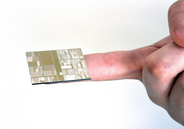
IBM Announces 7 nm Computer Chip Breakthrough


Chip
The latest breakthrough in technology seems to have overcome the main issue, which had posed one of the most "grand challenges" of the industry. IBM has created a test version of a semiconductor, which has the ability to shrink down the circulatry. This prototype is the first of its kind in the world. The microchip industry is always evolving and there are better products available in the market every new day. This ever evolving industry has to face immense difficulties due to the extent of their growth and due to various technological and physical limitations. But inspite of all the hindrances IBM has been successful in creating a chip with seven nanometers transistors.

Gradual advancement

The leader of this industry, Intel has been the recipient of several technical hurdles throughout. Technologists have even begun to question one of their foundation theories; they are questioning whether the long withstanding pace of chip improvement, the Moore's Law, could possibly continue beyond the present 14-nanometre generation of chips. Every generation of chip technology can be differentiated with the aid of the least size of fundamental component, which switches the current at nanosecond intervals. Now the advancement in technology has made the transition from the 14 nanometer to the manufacturing of 10-nanometer generation of chips.

Ever-evolving technology

This advanced technology created by IBM is basically an advanced version of the ultradense computer chips which has approximately four times the capacity of the other most powerful chips. As the advancements are brought forward in every generation of the chips, each of them brings forth an estimate of around 50% reduction in the region required by a given amount of circuitry. The new chips created by IBM are suggestive of a possibility that the semiconductor technology shall continue to shrink at least through 2018.

Individual identity

The advanced feature in these chips are the presence of the This advanced technology created by IBM is basically an advanced version of the ultradense computer chips which has approximately four times the capacity of the other most powerful chips. IBM has used silicon-germanium in their chips. In the other variants of chips, pure silicon is used. But IBM instead of using pure silicon has opted for silicon-germanium, which happens to be the key ingredient of the molecular-size switches. This also aids in faster transistor switching and in the lower power requirements.

Yet to be released in the market! 

However, it must be duly noted that most of these are mere speculations and experimentation. Nothing has been launched in the market as of yet. There are numerous complex procedures, which will test whether the product is viable for sale in the market. IBM shall take the final decision in collaboration with their development partners at the State University of New York's Polytechnic Institute in upstate New York. In the previous year, IBM had released a statement, which had declared their 3 billion dollars investment over a time period of five years to forward their chip technology and meet the demands of cloud computing, mobile products, data and other technologies.

Friday 10 July 2015

IBM Discloses Working Version of a Much Higher-Capacity Chip


IBM_Chip
IBM has taken the technology industry with surprise through its announcement of successfully developing working versions of ultradense computer chips. These chips are said to possess four times the capacity of today’s most powerful chips.

This announcement was essentially made on behalf of an international consortium led by IBM. IBM has invested $3 billion in an exclusive private public partnership in New York’s Hudson Valley with New York State, Samsung, GlobalFoundries and equipment vendors to manufacture advanced computer chips.

New Generation Of Chip In Development

It should be noted that each generation of chip is defined by the minimum size of fundamental components, which play role in switch current at nanosecond intervals. In modern times technology industry is actively working towards making a commercial transition from 14 nanometer to 10 nanometer manufacturing. Each generation helps in achieving 50 per cent reduction in the amount of area required for circuitry. IBM has affirmed its new chip which is still in research phase will be based on the shirking the area of semiconductor as much as possible by 2018.

IBM currently has working samples of chips with just seven nanometer transistors. It has been able to develop such sizes due to use of advanced silicon-gremanium instead of relying on pure silicon in key regions of chip. This material has made it possible to develop faster transistor switching with low power requirements, which is an added advantage. Given the smaller size of the transistors, it is highly possible to build microprocessors with not more than 20 billion transistors.

IBM Brings Focus Back On Itself As Revolutionary Chip Manufacturer

IBM has already shed a certain amount of its computer and semiconductor manufacturing capacity in the recent past. But this announcement shows that IBM is still interested in backing the technology manufacturing base with its efficient research facilities. Rather than being the horse power in building and providing chips to the companies it will act as a pioneer in unearthing advanced technological solutions for others. IBM will have to grapple with shift to use extreme ultraviolet (EUV) light for etching patterns on the chips at a resolution which approaches the diameter of an individual atom.

IBM will be licensing the technology to a variety of manufactures and most importantly, GlobalFoundries which is owned by the Emirate of Abu Dhabi will be making these chips for some big companies which includes, Qualcomm, Broadcom and others. It is yet to been whether semiconductor industry thinks on using silicon-gremanium as the best option or not.

IBM Refuses To Confirm Commercial Manufacturing


IBM has simply declined whether it will begin commercial manufacturing of this technology or not. Another ambitious company named Taiwan Semiconductor Manufacturing Company had given green lights to its plans to begin production of seven nanometer chips in 2017.

Given the precision required for using EUV light to keep the high capacity usage of chips optimum might be a concern in the commercial manufacturing operations. The goal of IBM here is to create next generation circuits, which offer higher capacity with reduced area, and most probably with current advancements and right amount of further research this technology will be introduced next year.

Thursday 5 February 2015

IBM Identity Mixer Wants To Better Protect Your Personal Data from Hackers


IBM Identity Mixer
IBM had finally developed a cloud-based cryptogram called Identity Mixer which will address the prevalent data breaches and theft in its own way. Identity Mixer would provide a safe haven for the users and it would keep them safe from any unwanted event of loss of personal data in any manner. This service is also going to make sure that suspicious and unwanted individuals don’t have access to the sensitive personal information.

In the years there had been several instances of loss of personal data such as in Home Depot, JPMorgan Chase and icloud hacking activities. Personal data today comprises of vast number of info which ranges from email address, phone numbers o credit card details. IBM Identity Mixer will help them securing those data in encrypted form.

Identity Mixer Could Help In Securing Personal Data To Great Extent

Identity Mixer provides solutions to the users in terms of giving out their personal data to different institutions in effective manner. It effectively uses the cryptographic algorithm which confirms automatically the user’s identity i.e. ‘who they are’ to the institution they wish to confirm without actually giving up personal information by themselves.

To across this dynamic solution straight forward lets consider that a person wishes to subscribe to a Netflix account. Netflix have it own terms and conditions such as users should be 18 years of age as well as live in a certain region in order to create an account. Identity Mixer comes in rescue for the users by providing an encrypted ID card which stores the personal information to such institutions without user’s requirement to do it manually.

Benefits Of Utilizing Identity Mixer

Identity Mixer will eliminate the need for the IT organisations to collect the personal information like age, nationality, address and most importantly the credit card numbers. Instead of manually declaring the data users will have a set of encrypted credentials in place which could be verified by Identity Mixer. This approach would also eliminate the use of sharing personal information by the users and at the same time it makes the process of identifying the user identities for any service provider on Web sphere. Identity Mixer is already working with AU2EU.

The Identity Mixer’s cryptogram could work with any other service which requires any kind of identification like the digital wallets which are gaining popularity these days. Having the Identity Mixer in place will make sure that user’s don’t have to input their credit card details into the digital wallets at all. In this respect this service also identical to the security system place in Apple Pay.

IBM To Enhance Its Identity Mixer

Currently IBM is running the public beta version of Identity Mixer on its state of art Bluemix cloud platform. But IBM has plans to make its Identity Mixer available to any provider of web service either through its own Bluemix or in the form of software deployed on their systems. IBM is even allowing the independent developers to try their hand on its Identity Mixer to make it better with new feature and highly secure in every aspect.


Friday 16 May 2014

IBM’s Replacement for NAND


IBM
New Project Theseus of IBM has some promising and capable ways of replacing the NAND in the long term with a widely higher performance together with better write endurance which would make this technology an excellent choice in storage if someone agrees in the manufacture of the same. IBM had portrayed a new way of memory technology which the company considers to be a replacement for NAND flash someday, and the company’s Theseus Project which is conducted in coordination with the University of Patras in Greece seems to be the first attempt in combining phase change memory, conventional NAND and DRAM on a single controller. The outcome is a hybridized storage solution which outperforms PCIe based SSDs between 12 and 275 times.

Physics of Phase Change Memory

The physics of phase change : The phase change memory is one of those alternative memory structure which has been proposed as a kind of replacement for NAND and the phase change memory operates by rapidly heating chalcogenide glass, moving it between it crystalline and amorphous state. While in its amorphous state which is read as binary 0, the structure has a very high resistance and in its crystalline state which is known as binary 1, the resistance is comparatively low. Phase change memory has the capabilities of quickly shifting between the two state and research done from Intel and Micron have also demonstrated the feasibility of intermediate states that enables two bits of information which can be stored in each cell.

Hybrid Structure for Effective Leverage

Moreover phase change memory has a much lower latency than NAND with a much faster read, write times in theory, and can tolerate millions of write cycles when compared to30,000 high end SLC NAND as well as few as 1,000 with TLC NAND. Besides, it is also well positioned compared to various other theoretical memory devices and NAND flash has huge economies of scale with billions invested in fab plants all across the globe. IBM along with Theseus has incorporated a small amount of PCM into a hybrid structure for effective leverage with its ultra-low latency characteristics.

3D NAND Better Choice

These early PCMs were built on a 90 nm CMOS at very low density where modern NAND flash is available presently in 512Gbit size when compared to 128Mbit for PCM. It is a compact order of magnitude which is faster than a commercial NAND accompanied with superior write performance with data longevity. Though there lies a problem where IBM makes a point that its PSS solution utilises 90nm memory which is produced by Micron, who earlier this year gave notice that it would be cancelling all of its PCM production and would be pulling out of the industry, while leaving the door open to revisit the memory tech sometime in the near future, they also indicated that the superior scaling of a 3D NAND would be a better choice inspite of the various problem faced with the technology in short term.

PCM – Promising Next Generation Memory Technology

According to 2013 ITRS report, it was noted that NAND performance was not expected to increase much from its present situation but in fact would be a bit difficult in maintaining current NAND performance while making improvement in density and holding write endurance constant. Presently PCM seems to be a promising next generation memory technology and someone needs to step in the manufacture of it or else it would be a difficult sell.

Friday 28 March 2014

Nvidia unveils Pascal, its next-gen GPU

Pascal
Pascal a super computer module was unveiled by Jen Hsun Huang, CEO of Nvidia, at the annual conference of the company. This new architecture optimizes data transfer between the CPU and the GPU and uses a new type of memory arranged in three dimensions. According to NVidia, the module presented, which is one third the size of a PCIe graphics card brings the power of a supercomputer in the area occupied by two credit cards.

 NVidia, the manufacturer of graphics processors for computers and systems on a chip (SoC) that is found in tablets and Smartphones, held its annual conference this week (CWG 2014) in San Jose, California. This is an opportunity to unveil new graphics processor architecture for the next generation of chips, video games, mobile SoC devices and supercomputers. Pascal called in honor of the French scientist Blaise Pascal, this super computer is an important technical milestone with the introduction of several technologies that optimize the use of RAM and reduce bottlenecks for data transfer between the GPU and the central processor CPU.

The first of these is the new 3D memory, which consists of stacked DRAM cells arranged vertically and integrate all on the same semiconductor as the CPU. NVidia announces that the memory should be multiplied by 2.5 with a much larger bandwidth. This 3D architecture also allows you to place voltage regulators near the chip, which has the effect of optimizing the energy efficiency that would be four times higher than a GDDR5 memory solution. NVidia emphasizes that through this, the Pascal module will have one third of the size of a PCIe graphics card.

For its new processor architecture, NVIDIA opted for a RAM in 3D. The memory access is much faster while allowing a more compact design. Another key innovation is a new interconnected technology between the CPU and GPU named NVLink. It was co-developed with IBM with the goal to leverage the speed of data transfer between the two processors. According to NVidia , NVLink is 5-12 times faster than that can offer PCI Express bus third generation, because it leaves the GPU memory access the CPU at full bandwidth and vice versa.

The founder announced a bandwidth of 80 to 200 Gb / s, against 16 GB / s of PCIe 3.0. NVLink also renews the interconnection between the GPUs themselves, which will make creating clustering configurations that may include multiple GPUs. This new type of interconnects will greatly benefit applications that take advantage of hardware acceleration and massively for parallel computing. Through this system of unified memory, NVidia promises developers they will be released for optimizing problematic communication protocols.

IBM plans to integrate this technology into future versions of Power processors. Note that NVidia does not intend to abandon the PCIe bus. All transactions and configuration control initiated by the CPU go through a PCIe connection only. If a CPU is not NVLink supported, may interconnect between the GPU and function to improve the performance rise, or scaling. In other words, NVLink will somehow technical manufacturers of processors may or may not choose to adopt. The first chips from the architecture Pascal arrive in 2016.

Monday 4 November 2013

Watson, the smartest IBM computer to diagnose the cancer better than medical students!


IBM Watson
Watson is simply the smartest computer in the world. Designed by IBM; which is endowed with more artificial intelligence, that is capable of diagnosing cancers with a success rate higher than that of the medical students. It is a revolution in the medical world which is brought by Watson.

Its new mission is now to come and help doctors at Memorial Sloan -Kettering Cancer Center in New York, a center that has treated 1125 patients with a lung tumor in 2012. For this, a team of 25 researchers helped artificial intelligence to assimilate more than 600,000 medical data, primarily lung cancer.

The computer is now able, thanks to its ability to understand natural language, not computer language, to respond to questions from doctors and diagnose with a success rate of 90% of lung cancer! By downloading the patient record in the machine, Watson informs the doctor about the best treatment to use and displays a ranked list according to a confidence index decreasing.

Watson is currently undergoing testing in a New York hospital. Thanks to him, health care costs could be reduced by 30 % in the United States, either one, € 46 billion! The technology of artificial intelligence that is simply extraordinary and we hope it can help many people. In fact many are fascinated by this technological advancement but others prefer to rely on the advice of doctors.

Saturday 4 May 2013

IBM Makes a Movie Out of Atoms with Microscope


The Big Blue crew managed to make a film by moving atoms of carbon monoxide, visible through a microscope capable of magnifying 100 million times. When IBM researchers in storage decide to film, the means are rather original ... Big Blue has managed the feat effect of creating a short film based animated atoms. In this short film ("A Boy and his Atom"), where you can see a boy playing with a ball and jump trampoline, are 5000 atoms of carbon monoxide that were used. Specifically, the U.S. giant has used a scanning tunneling microscope, camera effect that allows you to see the world of the infinitely small to the atoms. This device allows you to magnify objects 100 million times.

The atoms were then positioned to form the schematic image of the boy in the image of single pixels. Engineers used a very fine needle to move atoms and film frame by frame (stop-motion). "The ability to control the temperature, pressure and vibration to very specific levels that the IBM research laboratory one of the few places in the world where the atoms can be moved with such precision," said Christopher Lutz of IBM. Why did you make this "movie"? This is done for IBM to demonstrate its ability to manipulate atoms on magnetic media in optical data storage the IBM replied. Until this technology is declined storage, IBM has seen his film to be entered in the Guinness Book of Records as the "world's smallest film."